
Application of Short Wave Infrared (SWIR) Technology in Various Fields
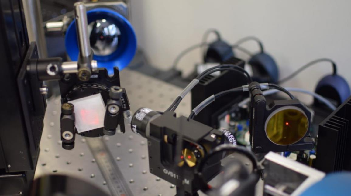
Shortwave Infrared (SWIR) cameras detect invisible product defects and specific material properties, opening up a wide range of applications for machine vision solutions: compared to mainstream machine vision cameras with CMOS or CCD sensors, most SWIR cameras are equipped with InGaAs (Indium Gallium Arsenide) sensor with detection wavelengths between 900nm and 1,700nm.
The newest sensors extend their supported spectral range to the visible spectrum, or beyond 1,700nm, up to 2,500nm. Light with wavelengths beyond 750nm belongs to the spectrum invisible to the naked eye, and traditional CCD or CMOS cameras can only detect light with wavelengths below about 1050nm. Therefore, SWIR cameras have a wider range of applications than conventional cameras, for example, they can easily detect water accumulation inside plants or defects inside wafer products.
This article presents examples of applications of SWIR cameras in various fields, such as the semiconductor industry, recycling and agriculture, and airborne remote sensing. Since some SWIR cameras are primarily designed for research facility applications, they need to provide not only the high image quality necessary for industrial applications but also an industrial-grade rugged design and camera features commonly used in machine vision applications.
Semiconductor industry
The semiconductor industry has grown into one of the largest industries in the world, and the growth momentum continues unabated. Wafer integrated circuit (IC or chip) production is the core business of the industry.
Cameras with InGaAs sensors typically operate in the short-wave infrared spectral range from 900nm to 1,700nm and can achieve spectral imaging at wavelengths around 1,150nm through semiconductor materials such as silicon (Si). Therefore, short-wave infrared cameras have become indispensable equipment in the inspection process. Transparency imaging of silicon wafers is a non-destructive inspection method that offers many benefits to the production process. Today, the semiconductor industry is introducing InGaAs cameras into the test, inspection, and quality control systems.
Photovoltaic power generation
From silicon crystals to ingots/bricks, wafers, solar cells, and even solar modules, SWIR camera applications cover the entire supply chain inspection process. Since a camera equipped with an InGaAs sensor can achieve light-transmitting imaging of silicon-based materials, it is the most effective solution for detecting internal physical defects in silicon-based materials.
In addition to the newly emerging short-wave infrared imaging inspection technology, other important technologies and methods commonly used in the photovoltaic industry include photoluminescence (PL) and electroluminescence (EL) two commonly used inspection methods.
PL imaging utilizes optical excitation (such as laser irradiation) to generate electron-hole pairs, which induce emission through radiative recombination, thereby triggering camera-sensitized imaging. The interband emission of around 1,150nm provides information about the internal defects and dislocation clusters in silicon-based materials. In addition, by mapping the defect band emission at about 1,550nm, results on the ultimate cell efficiency limit can be obtained. Therefore, InGaAs cameras with high detection sensitivity in the 900nm to 1,700nm range are ideal for such applications.
Electroluminescence is the result of radiative recombination of electrons and holes in silicon-based materials. The technique applies a voltage to the solar cell, recombines with available holes, and finally emits photons according to the bandgap of the absorber (silicon 1,150nm).
In addition to crystalline silicon, other types of solar cell or module materials (also known as thin-film solar cells) can be inspected using this technique: 700nm to 1,330nm (depending on the indium/gallium ratio) wavelength range inspection of copper indium gallium diselenide (CIGS); 1,330 nm wavelength range to examine copper indium diselenide (CIS).
The main advantages of SWIR compared to CCD and CMOS cameras are shorter exposure times and excellent quantum efficiency (QE) in the silicon dominant emission wavelength range, ensuring rapid identification in the production process. CCD or CMOS cameras require longer exposure times, up to 30 seconds. Even with NIR-enhanced CCD sensors, the exposure time required is 3 seconds or more. The SWIR camera, on the other hand, only takes a few milliseconds, which can greatly increase productivity.
Recycling industry
The amount of waste generated in developed countries is growing while the number of available resources is becoming increasingly scarce; therefore, it is necessary to develop effective methods to separate high-quality recyclable materials from collected waste.
Plastic sorting
Since the visible spectrum of all plastic waste is broadly similar, it is not possible to separate the recyclable material by conventional methods. However, in the short-wave infrared range, the absorption spectra of different plastic materials exhibit different characteristics. Therefore, we can build an automated separation system with the help of short-wave infrared camera technology to separate and recover materials of similar quality and properties. The latest version of the SWIR camera extends the spectral range to 2.5µm and can distinguish more material types.
To achieve an efficient automated waste separation process, the material is first to cut into small flakes of similar size. The sheets are then transported by means of a conveyor belt to an inspection system consisting of an illumination system and a short-wave infrared camera with an InGaAs sensor.
Since different plastic materials exhibit different spectral properties in the short-wave infrared, this property can be used to differentiate between different materials, and the corresponding plastic-type can be assigned based on the spectral properties. On the conveyor belt, the different types of plastic are separated by a series of air jets. This step can be repeated multiple times to achieve fine separations with good recoveries and high-quality results.
Food industry
Fruits and vegetables contain 80 to 90 percent water. Therefore, its spectral response characteristics are mainly reflected in the water absorption band, with a peak at about 1,450nm. Due to its strong light-absorbing ability, the imaging results of water in the short-wave infrared band are significantly darker.
Agriculture
Spectral imaging can also be used for agricultural purposes, especially when used with unmanned aerial vehicles (UAVs). Farmers can use this technology to inspect crops remotely, such as strawberry fields: by looking at short-wave infrared images, plants or areas that are deficient, have just the right amount of moisture, or have too much moisture can be identified. The higher the detected moisture content, the higher the absorption peak at 1,450nm wavelength and the darker the corresponding area in the image. Therefore, such applications typically use a narrower 1450nm bandpass filter to enhance this effect.
Airborne remote sensing
Drones are particularly common in agriculture, but can also be used for other purposes, such as inspecting a variety of materials from the air. Each inorganic material has a unique chemical composition and crystal structure, resulting in a unique spectral response corresponding to its specific light absorption properties.
Geological and mineral inspection
Through the unique spectral response, the distribution of minerals around the world can be mapped. In addition, forestry companies can use this technology to map forest land. Hyperspectral imaging can aid in geological and mineral exploration using methods similar to food analysis.
In conclusion
SWIR cameras with InGaAs sensors are powerful and have gained widespread popularity and general acceptance in the machine vision market over the past five years. It is especially appreciated that these cameras today support the same machine vision standards as mainstream visible light cameras, such as GigE Vision or GenICam. This feature helps greatly ease system integration and ensures that the SWIR imaging system is ready for immediate use after installation.
In the future, the application field of short-wave infrared cameras will be further expanded, and the development of sensor technology will play an important role in it. In rare cases, only one camera can be used for some applications, and sensors extending beyond the visible spectral range (400nm-1,700nm) can help reduce system complexity. Cameras with SWIR sensitivity extended to the 2,500nm range can detect other types of materials or features. Finally, sensors with smaller pixel sizes can also capture objects at higher spatial resolution and at a lower cost.
The above introduces the application of short-wave infrared (SWIR) technology in various fields. If you want to buy a short-wave infrared imaging camera, please contact us.
JAVOL is a professional custom infrared imaging equipment manufacturer. Relying on the multi-spectral high-sensitivity photoelectric sensor chip of advanced compound semiconductor materials, with deep learning AI algorithm as the engine, integrating low-light night vision technology, infrared thermal imaging technology, short-wave infrared technology, and multi-spectral fusion technology, our company designs, develops and manufactures Advanced imaging products and system solutions are widely used in machine vision, autonomous driving, drone payloads, high-end manufacturing, and medical diagnosis.