
How to Use a Short-wave Infrared Camera to Detect Silicon Wafer Defects?
Electronic equipment has become very common in today's modern technology. Everyone may have encountered and used silicon wafers indirectly when using electronic equipment. The wafer is a thin semiconductor material substrate used to manufacture electronic integrated circuits. There are various types of semiconductor materials, and the most commonly used semiconductor material in electronic devices is silicon (Si).
Silicon wafers are a key part of integrated circuits. It is made by slicing high-purity, almost defect-free single crystal silicon rods, and is used as a substrate for manufacturing microelectronic devices in and on the wafer surface. Wafers can be made through multiple micromachining process steps, such as masking, etching, doping, and metallization.
Integrated circuits (ICs) have become the main components of almost all electronic devices. IC is a process of transplanting and printing a large number of microstructures of electronic circuits and components onto the surface of a semiconductor crystal (such as silicon). Components, circuits, and substrates are all fabricated on a single wafer. Hundreds of integrated circuit ICs can be manufactured on a single thin silicon wafer at the same time, and then divided into multiple individual IC chips.
Silicon wafers will accumulate residual stresses during growth, cutting, grinding, etching, and polishing. Therefore, silicon wafers may have cracks throughout the manufacturing process. If the cracks are not detected, those wafers containing cracks will produce useless products in the subsequent production stages. Cracks may also occur when the integrated circuit is divided into individual ICs.
Therefore, in order to reduce manufacturing costs, it is very important to inspect the raw material substrate for impurities, cracks, and defects during processing before further processing. JAVOL gave you a detailed introduction to the method of detecting silicon wafer defects using an infrared camera.
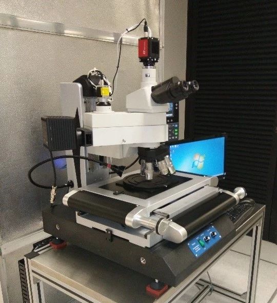
Figure 1: Silicon wafer defect inspection system equipped with an AVT SWIR camera
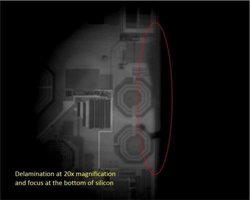
Figure 2: Defects detected in silicon wafers
Silicon has the characteristic of being able to transmit infrared rays. Therefore, the indium gallium arsenide (InGaAs) camera is suitable for the SWIR (Short Wave Infrared) wavelength range from 0.9µm to 1.7µm, allowing users to see through semiconductor silicon substrates. The characteristics of shortwave infrared penetrating semiconductor materials have brought great benefits to the manufacturing process of semiconductor materials. Infrared images can highlight defects (cracks) inside the silicon wafer.
It is very simple to use SWIR cameras to detect internal defects of wafers and integrated circuit chips because these materials (silicon Si and gallium arsenide GaAs) are transparent in the short-wave infrared wavelength range. This ability to see through silicon materials provides a non-destructive testing method, which greatly improves the production process.
During the wafer manufacturing process, there may be particles or cracks inside the wafer or between the wafers. The CCD or CMOS camera used in the visible light band can only be used to detect defects on the top of the wafer, while the SWIR camera can see the inside of the silicon material and can detect particles, gaps, and other defects between two bonded wafers.
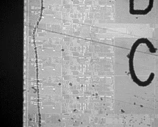
Figure 3: SWIR camera shooting-internal cutting damage of silicon material
Die inspection before packaging is also a common application of SWIR cameras because SWIR cameras can see small cracks hidden inside the silicon material caused by wafer cutting. (Figure 4)
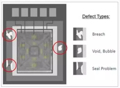
Figure 4: SWIR image shows seal failure
SWIR cameras are used to increase the output of MEMS manufacturing: seal inspection (to detect foam or damage, see Figure 4), device defect inspection, critical dimension, and overlay measurement. For wafer-level packaging (WLP), combined with wafer manufacturing technology and equipment packaging technology, SWIR cameras are used for a variety of quality assessment tasks.
Shortwave infrared (SWIR) cameras are used in infrared microscopy imaging to detect defects in the semiconductor manufacturing process. If you want to learn more about SWIR cameras after reading the above, you can get a comprehensive solution by contacting us.
With its leading R&D technology and excellent manufacturing process, JAVOL has become a leader in the infrared thermal imaging system manufacturing industry. We are committed to providing users with high-quality products and thoughtful services. We are equipped with a professional quality inspection system and a comprehensive management system, which can fully control the quality and details of the products. At the same time, we will also provide effective solutions according to the diverse needs of users. If you are interested in our SWIR cameras, please contact us immediately!